
A calculated decision
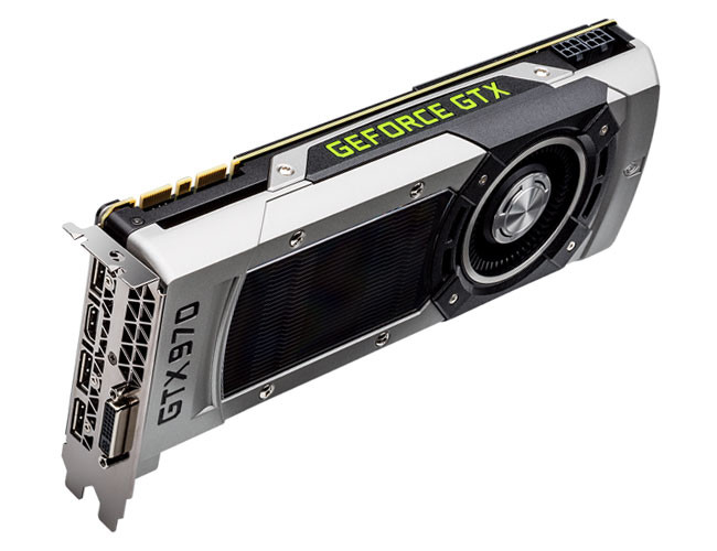
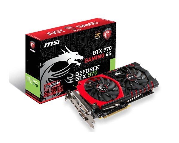
By a stroke of good fortune and beneficial planetary alignment, I was able to acquire an MSI GTX 970 a few days ago and I have to say that this GPU has exceeded my expectations and then some. I was previously sporting a Sapphire Radeon 7950 3Gb, which in itself is no slouch and the performance increase in games such as Dying Light, Far Cry 4 and Crysis 3 with the new GTX 970 is awesome. Before I grabbed the new card, I had a good look at the Radeon 280X, which is really a re-badged 7970, but in the end, shiny toy-shop syndrome got the better of me, so I jumped ship and headed over to Nvidia. I’m not what you might call a fanboy of either AMD or Nvidia, as over the years I’ve used both brands in equal measure. In fact my first major GPU upgrade from 3dfx was a Gainward Geforce 3 64Mb which I still have kicking about somewhere. However, AMD always appeared to offer more bang for buck over the recent years of austerity, but it was time for a major upgrade this time round, especially as the latest games are now so demanding on your hardware.
I came across the issue of the GTX 970 memory design a few days before deciding to buy it and, reasoning that I won’t be going SLI and that 4K will be beyond my reach for some time to come, I made a calculated decision, sort of.
What’s the big deal?
When Nvidia launched the GTX 970 in September last year, it was billed as next generation using the new Maxwell architecture complete with 4Gb of DDR5 VRAM and if you blinked you’d probably not have noticed that Nvidia also published the ROP’s (render output units) at 64, and level 2 cache at 2Mb. Now that kind of detail may have been lost on many users, myself included, where many of us look for power consumption, core clock speed, amount of processing units and total amount of VRAM. It transpires that the figures initially quoted were NOT correct and the real figures are as shown in the following chart:
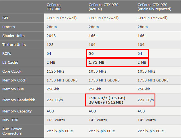
The memory usage or segmentation is the most significant factor here and if a game demands VRAM in excess of 3.5Gb, it will utilise the slower 512Mb at 24Gb/s as opposed to the originally stated 224Gb/s for the entire 4Gb VRAM, possibly resulting in drastic reduction in frames per second (FPS) rendered. This alleged misrepresentation of the actual GTX 970 specification has resulted in a class-action lawsuit in the Northern District of California.
According to the plaintiffs, Nvidia “engaged in a scheme to mislead consumers nationwide” and that the company “misrepresented” key selling points of the device. Erm, I would have to ask about the rest of us, being worldwide buyers, but of course that would be a case of jurisdiction.

Nvidia has responded by saying that the 3.5Gb/512Mb VRAM segmentation will have minimal impact on gaming and that the engineering design and setup are a feature of this card. In fact Nvidia CEO Jen-Hsun Huang has responded in the Nvidia blog…
GTX 970 is a 4GB card, however, the upper 512MB of the additional 1GB is segmented and has reduced bandwidth. This is a good design because we were able to add an additional 1GB for GTX 970 and our software engineers can keep less frequently used data in the 512MB segment.
and further on….
This new feature of Maxwell should have been clearly detailed from the beginning.
We won’t let this happen again. We’ll do a better job next time.
Gamers’ reactions
As you would expect, there’s been a mixed response to both the false advertising allegations and the response from Nvidia. Many gamers are furious that they’ve been sold a pup; many are saying they’ve been lied to and thousands have signed online petitions demanding a refund. As for Nvidia’s response, the general attitude from many gamers is ‘Well, they would say that wouldn’t they!’ I won’t reproduce the comments here, but if you take a peek at the Geforce forums and all 370 pages on this topic, you should get a flavour of how many are feeling about this.

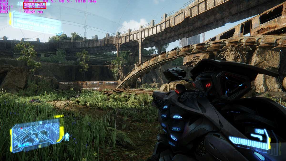
But the proof of the pudding is always in the eating, surely? For my part, I have no complaints about the GTX 970, it’s rock solid in every game at maximum graphic settings, which is not something I could achieve previously. I also enjoy testing the hardware and using an in-game overlay such as MSI Afterburner which can show some interesting real time statistics, such as FPS, memory usage and temperatures. In this case and pertinent to the GTX 970 issue, the memory usage is a crucial factor in determining whether we have in fact been duped and sold a pup, or the GPU is functioning as it was designed to do.
Take a look at this video of Assassin’s Creed, played using a highly specked machine which includes a GTX 970 with 4Gb of VRAM.
[youtube]http://youtu.be/PW3GdR4Gnzc[/youtube]
What I see is a highly textured game with superb graphics and if you look at the overlay in the top left corner (MEM not RAM), the memory usage is clearly hitting the 4Gb mark with no apparent loss in visual loveliness. Alright, he’s not showing the FPS but at least we get a fair representation of how the game looks with 4Gb memory usage, which is pretty damned good in my book.
Has the case got legs?
I’m not a lawyer, so I couldn’t really say either way. However, Nvidia clearly dropped a clanger here; there appears to have been a communication problem between engineering and marketing and believe me, if you’ve ever worked in manufacturing you’ll know that this can happen sometimes. The CEO hasn’t definitively apologised, meaning he hasn’t said sorry, but he has acknowledged the error and promised to do better next time. I don’t believe for one second that this was a deliberate ploy to deceive consumers, although if you read some of the comments written by gamers who used to be Nvidia fanboys, you’d be forgiven for believing that Nvidia was the new axis of evil and it was a deliberate ploy to shaft them. As far as I know, Nvidia have no plans to roll out a 970 specific patch or driver (if it were even possible), they are not encouraging people to return their graphic cards and they seem pretty adamant that the engineering set up of this card is the way they designed it to be.
As for the plaintiffs demands, one can only speculate as to whether they will see 5 million bucks, but of course that’s the nature of class-actions, big money. It’s pretty clear that Nvidia has always stated 4Gb as being the advertised amount of memory (which it is), but as to how it is allocated is a moot point. The ROPs and L2 cache? Well, one imagines that will be thrashed out by the clever use of semantics in some smoke filled room on the West Coast with sandwiches and coffee.

Will I be signing petitions, demanding a refund or knocking on Nvidia’s door asking for tea and sympathy? I think not, for all the reasons stated. That isn’t to say that some may not have a legitimate claim in very high resolutions above 1080p, but on the evidence I’ve seen so far, including tests on my own rig at maximum settings, this whole episode smacks of over reaction, fanboy tantrums, and much ado about nothing.
Finally, check out this video of Far cry 4 gameplay at a resolution of 3840 x 2400 (blimey!) and absolute maximum settings. The VRAM usage is almost entirely used throughout i.e the whole 4 Gb with no loss or stuttering whatsoever. It does look gorgeous doesn’t it?
[youtube]http://youtu.be/rxy4Ct7TZjw[/youtube]